What do computer chips reveal about the creativity of their designers
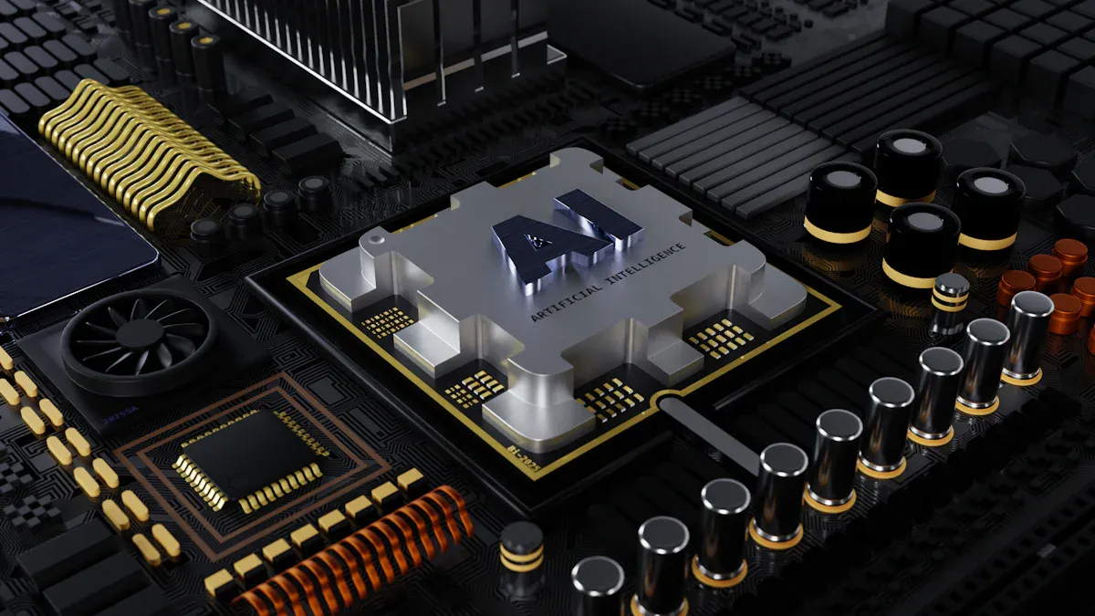
A computer chip often hides more than circuits and transistors. Designers embed playful doodles or unique design elements, revealing personal flair. Roughly 10% of chips, as noted by experts, contain these hidden artworks. These details offer a glimpse into the minds that shape modern technology.
Key Takeaways
- Computer chip designers hide tiny artworks and messages inside chips to express their creativity and leave a personal mark.
- Advanced fabrication tools let engineers add detailed designs without affecting chip performance, blending art with technology.
- These hidden features show the human side of engineering, inspiring innovation and connecting culture with modern technology.
How do computer chip designers express creativity?
What are chip "easter eggs" and hidden artworks?
Chip designers often embed "easter eggs"—hidden messages, images, or symbols—within the intricate layers of a computer chip. These secret features reflect a long-standing tradition in technology, where creators leave subtle marks as a form of personal expression. The concept of the "easter egg" originated in software, notably when Warren Robinett hid his name in the 1979 Atari game Adventure. This act protested the lack of developer recognition and inspired others to include hidden content in their work. The term itself emerged at Atari, describing these concealed surprises as akin to a treasure hunt.
Earlier examples predate the term, such as a hidden McDonald's restaurant in the 1973 video game Moonlander and playful responses in early computer commands. Over time, this tradition migrated from software to hardware, with engineers embedding tiny artworks, initials, or even cartoons into the unused spaces of a computer chip. These hidden elements rarely affect functionality but offer a glimpse into the designer's personality and sense of humor.
Note: Easter eggs in chips are rarely visible to the naked eye. Engineers often use electron microscopes to reveal these micro-scale artworks, making their discovery a special event for those in the know.
How do technical processes allow for artistic expression?
The process of creating a computer chip involves advanced fabrication techniques, such as photolithography, etching, and deposition. These methods enable the formation of intricate patterns at microscopic scales. Innovations like Deep Ultraviolet (DUV) and Extreme Ultraviolet (EUV) lithography allow for unprecedented miniaturization, making it possible to include detailed artistic elements at the micro or nanoscale. However, the environment in which chips are made imposes strict limitations. Even a tiny particle can cause device failure, so manufacturers prioritize cleanliness and process control. This focus on reliability restricts the size and complexity of any non-functional designs.
Despite these constraints, advances in lithography and fabrication technology have expanded creative possibilities. High-precision photolithography, automation, and AI-driven process control now enable more complex and compact chip designs. Engineers can use these tools to add creative features without compromising performance. For example:
- Extreme Ultraviolet Lithography (EUVL) achieves feature sizes below 10 nm, supporting intricate patterns.
- Directed Self-Assembly (DSA) allows for high-resolution, precise patterning at low cost.
- AI-powered Electronic Design Automation (EDA) tools automate repetitive tasks, freeing engineers to focus on innovation and creative problem-solving.
These advances collectively enhance the ability to add creative, complex, and high-performance features to a computer chip, while still meeting strict technical requirements.
Why do engineers include personal or playful elements?
Engineers often view chip design as a blend of art and science. Like architects, they balance functionality with aesthetics, innovating within practical constraints. The inclusion of personal or playful elements serves several purposes:
- Self-expression: Designers use hidden artworks to leave a personal mark, celebrating their role in a collaborative project.
- Team identity: Groups may embed logos, mascots, or inside jokes to foster camaraderie and pride.
- Innovation encouragement: Creative freedom, even in small ways, motivates engineers to push boundaries and solve problems in novel ways.
- Tradition: The practice of embedding easter eggs connects current designers with the pioneers of the field, maintaining a sense of continuity and shared culture.
AI-powered tools further support this balance by automating routine tasks, allowing engineers to devote more energy to creative and architectural innovation. By fostering an environment that values both technical excellence and creative expression, the industry encourages engineers to innovate while meeting deadlines and budgets.
Tip: The next time you use a device powered by a computer chip, remember that beneath its surface may lie a hidden signature, a tiny doodle, or a playful message—evidence of the creativity and humanity behind the technology.
What real-world examples of computer chip art reveal designer ingenuity?
Which famous computer chips feature hidden art or messages?
Many well-known chips contain hidden art or messages that showcase the playful side of engineering. Designers have embedded a variety of images and symbols into the silicon, often visible only under a microscope. Some notable examples include:
- A sundial on the Hewlett-Packard PA-7300LC microprocessor, symbolizing clock circuitry.
- A silicon space shuttle and the Starship USS Enterprise on Texas Instruments Schottky Logic integrated circuits.
- A slide trombone artwork on an AMD integrated circuit.
- A Tyrannosaurus rex driving a convertible sports car on the Digital Equipment Corporation Rigel chipset.
- A stork carrying a baby on the Motorola 68HC05PG microcontroller.
- A silicon Smurf pulling a wagon on a Siemens integrated circuit.
- A Mickey Mouse image on the Mostek 5017 alarm clock chip.
- A Pac-Man character on a TEMIC Semiconductors RF chip.
These examples demonstrate that the tradition of embedding art in chips spans decades and includes references to pop culture, humor, and personal interests.
How do personal and cultural influences shape chip art?
Personal and cultural backgrounds play a significant role in shaping chip art. Artists like Marilou Schultz blend traditional Navajo weaving techniques with the geometric patterns found on processor cores. This fusion connects cultural heritage with modern technology, adding depth and meaning to the artwork. The Navajo community’s history in semiconductor manufacturing, such as work at the Fairchild plant in Shiprock, New Mexico, further enriches the connection between regional identity and chip design. The deliberate pace of weaving contrasts with the rapid nature of digital technology, creating a unique artistic tension.
What motivates designers to leave their mark on computer chips?
Designers embed art or messages in chips for many reasons:
- They seek to express personal values and identity beyond technical function.
- Many challenge the focus on efficiency by adding subjective experiences to their work.
- Some aim to provoke reflection on the human element in technology.
- Others explore alternative narratives and aesthetics, influencing mainstream design.
- Artistic exploration and social critique inspire them to enrich daily life through technology.
- Collaborations with artists and social scientists help create technology that is socially and culturally meaningful.
Note: These creative acts transform the computer chip from a purely functional object into a canvas for innovation and self-expression.
Why do creative acts in computer chip design matter?
What do these details reveal about the human side of engineering?
Creative acts in chip design reveal the emotional and cultural dimensions behind technical achievements. Interviews with industry leaders show that engineers often face challenges that require flexibility and adaptability. For example, they must navigate new technologies and overcome resistance to change, especially when adopting AI-driven methods. These stories highlight the perseverance, passion, and collaboration that drive innovation. Engineers do not just solve technical problems; they bring their personalities, values, and creativity into every computer chip they design.
How does chip art bridge the gap between art and technology?
Chip art serves as a unique bridge between artistic tradition and technological innovation.
- It connects artisans from diverse backgrounds to the digital world, allowing them to share cultural stories through technology.
- Virtual workshops and augmented reality experiences enable direct communication between creators and audiences.
- Artistic techniques, such as using vibrant dyes on microfluidic chips, transform scientific tools into visually stunning works of art.
This blending of disciplines empowers communities and preserves heritage, while also making technology more relatable and engaging.
What can we learn about innovation and self-expression from these hidden features?
Hidden features in chip design inspire future generations of engineers to combine creativity with technical expertise.
- AI tools automate routine tasks, freeing engineers to focus on innovation.
- Generative design approaches encourage unconventional thinking and new architectures.
- Human-AI collaboration accelerates development and democratizes chip design.
These trends show that innovation thrives when engineers embrace self-expression and creative problem-solving. The computer chip becomes more than a tool; it becomes a testament to human ingenuity and the evolving partnership between people and technology.
Creative details hidden in chips reveal the ingenuity and spirit of their designers.
- Vertical stacking, in-house design, and cloud-based workflows reflect broader innovation trends.
- Projects blending engineering and art, like sensory devices and robotic drawing, highlight the synergy between disciplines.
Silicon doodles and artistic interpretations preserve the legacy of these creators, humanizing technology for future generations.
FAQ
What tools help engineers add art to computer chips?
Engineers use advanced design software and photolithography equipment. These tools allow precise placement of tiny images or messages within the chip’s layers.
Can chip art affect a chip’s performance?
Chip art usually stays in unused areas. Designers ensure these features do not interfere with the chip’s function or reliability.
Why do people rarely see chip art?
Most chip art appears at microscopic scales. Only specialized equipment, such as electron microscopes, can reveal these hidden details to the human eye.